
Introduction to SEM in Material Characterization
Material characterization remains a fundamental requirement across multiple scientific and industrial fields. Despite advances in computational modeling and numerical simulation, experimental validation is still essential. Accurate prediction of material behavior depends on reliable physicochemical parameters, which must be obtained through advanced analytical techniques.
Characterization can take multiple forms:
- Morphological analysis: surface state, topography, grain size, fractures, and porosity
- Chemical analysis: phase identification, impurities, and inclusions
- Crystallographic analysis: structural orientation and phase distribution
Among modern analytical tools, Scanning Electron Microscopy (SEM) has become a key technique, particularly for high-resolution surface imaging and microstructural analysis.
Fundamental Concept of Scanning Electron Microscopy
SEM is an advanced imaging technique that uses a focused electron beam to scan the surface of a sample. The interaction between the electron beam and the material generates various signals, which are detected and transformed into high-resolution images.
The term:
- Electron: refers to the use of accelerated electrons instead of light
- Scanning: describes the systematic movement of the beam across the sample surface
This process enables the reconstruction of detailed images with:
- Spatial resolution below 5 nm (and down to ~0.5 nm in modern systems)
- High depth of field, providing a 3D-like surface visualization
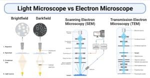 From Optical Microscopy to Electron Microscopy
The resolution of optical microscopy is fundamentally limited by the wavelength of visible light (~200 nm). To overcome this limitation, electron microscopy uses electrons with much shorter wavelengths.
According to the wave-particle duality principle, the wavelength of electrons decreases as their ऊर्जा increases, allowing observation at the nanometer scale.
Key advantages over optical microscopy:
- Significantly higher resolution
- Ability to observe nanoscale structures
- Enhanced depth of field
This technological breakthrough led to the development of electron microscopes in the early 20th century, revolutionizing imaging at the atomic and nanometric levels.
Principle of Operation
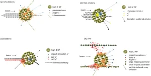
When an electron beam interacts with a solid sample, multiple interactions occur:
Types of interactions
- Elastic interactions → electron scattering and trajectory changes
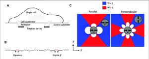
- Inelastic interactions → energy loss, excitation, and ionization
SEM detects a variety of signals, including:
- Secondary electrons (SE) → surface topography
- Backscattered electrons (BSE) → compositional contrast
- X-rays (EDS/WDS) → elemental analysis
- Cathodoluminescence → optical properties
- EBSD patterns → crystallographic orientation
The detected signal intensity modulates the brightness of each pixel, forming the final image.
Advanced Analytical Capabilities
SEM is not limited to imaging. It integrates multiple analytical techniques:
- Energy Dispersive Spectroscopy (EDS) → elemental composition
- Wavelength Dispersive Spectroscopy (WDS) → precise chemical analysis
- Electron Backscatter Diffraction (EBSD) → crystallography
- 3D reconstruction → layered structure analysis
These capabilities make SEM a multifunctional platform for both imaging and microanalysis.
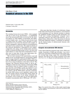
Instrumentation and Image Formation
SEM imaging relies on the synchronization between:
- The electron beam scanning the sample
- The signal detection system
- The display system
Image quality depends on:
- Beam diameter
- Signal intensity
- Signal-to-noise ratio
- Scanning speed
Noise in SEM images originates from:
- Random electron emission
- Detector and electronic system limitations
Modern SEM systems reduce noise through:
- Signal filtering
- Image averaging
- Optimized scanning conditions
 Technological Evolution of SEM
Since its development in the mid-20th century, SEM technology has evolved significantly:
- Field Emission Guns (FEG) → improved resolution at low voltage
- Environmental SEM (ESEM) → imaging of hydrated and non-conductive samples
- Dual-beam systems (FIB-SEM) → imaging + micro-machining
- Tabletop SEM → compact, user-friendly systems
Automation and digital imaging have further enhanced usability and analytical performance.
Advantages and Limitations
Advantages
- High spatial resolution (~1 nm)
- Wide magnification range (×10 to ×100,000+)
- Exceptional depth of field (3D-like images)
- Minimal sample preparation
- Combined imaging and chemical analysis
- Broad application fields (materials science, biology, nanotechnology)
Limitations
- Requirement of vacuum environment
- Possible sample damage due to electron beam
- Challenges with non-conductive or sensitive samples
- Risk of image artifacts and misinterpretation
Applications of SEM
SEM is widely used across multiple disciplines:
- Materials science → metals, ceramics, polymers
- Nanotechnology → nanoparticles and nanostructures
- Biology → cells and tissues
- Electronics → semiconductor inspection
- Failure analysis → fracture and defect investigation
Conclusion
Scanning Electron Microscopy is a powerful and versatile analytical technique that combines high-resolution imaging with advanced material characterization. Its ability to provide detailed topographical, chemical, and crystallographic information makes it indispensable in modern research and industry.
Continuous technological advancements particularly in automation, detector systems, and electron optics are driving SEM toward higher precision, improved accessibility, and broader applications in nanoscience and beyond.